

IGBT
IGBTwithintegrateddiodeinpackagesofferingspacesavingadvantage
IKD15N60RA
600VTRENCHSTOP
TM
RC-Seriesforhardswitchingapplications
Datasheet
IndustrialPowerControl

2
IKD15N60RA
TRENCHSTOP
TM
RC-Seriesforhardswitchingapplications
Rev.2.1,2013-02-15
IGBTwithintegrateddiodeinpackagesofferingspacesavingadvantage
Features:
TRENCHSTOP
TM
ReverseConducting(RC)technologyfor600V
applicationsoffering
•OptimisedV
CEsat
andV
F
forlowconductionlosses
•SmoothswitchingperformanceleadingtolowEMIlevels
•Verytightparameterdistribution
•Operatingrangeof1to20kHz
•Maximumjunctiontemperature175°C
•Shortcircuitcapabilityof5µs
•Bestinclasscurrentversuspackagesizeperformance
•QualifiedaccordingtoAECQ101
•Pb-freeleadplating;RoHScompliant(forPG-TO252:solder
temperature260°C,MSL1)
CompleteproductspectrumandPSpiceModels:
http://www.infineon.com/igbt/
Applications:
•HIDlighting
•Piezoinjection
G
C
E
G
E
C
KeyPerformanceandPackageParameters
Type
V
CE
I
C
V
CEsat
,T
vj
=25°C
T
vjmax
Marking
Package
IKD15N60RA
600V
15A
1.65V
175°C
K15R60A
PG-TO252-3

3
IKD15N60RA
TRENCHSTOP
TM
RC-Seriesforhardswitchingapplications
Rev.2.1,2013-02-15
TableofContents
Description . . . . . . . . . . . . . . . . . . . . . . . . . . . . . . . . . . . . . . . . . . . . . . . . . . . . . . . . . . . . . . . . . . . . . . . . 2
Table of Contents . . . . . . . . . . . . . . . . . . . . . . . . . . . . . . . . . . . . . . . . . . . . . . . . . . . . . . . . . . . . . . . . . . . 3
Maximum ratings . . . . . . . . . . . . . . . . . . . . . . . . . . . . . . . . . . . . . . . . . . . . . . . . . . . . . . . . . . . . . . . . . . . . 4
Thermal Resistance . . . . . . . . . . . . . . . . . . . . . . . . . . . . . . . . . . . . . . . . . . . . . . . . . . . . . . . . . . . . . . . . . 4
Electrical Characteristics . . . . . . . . . . . . . . . . . . . . . . . . . . . . . . . . . . . . . . . . . . . . . . . . . . . . . . . . . . . . . . 5
Electrical Characteristics diagrams . . . . . . . . . . . . . . . . . . . . . . . . . . . . . . . . . . . . . . . . . . . . . . . . . . . . . . 8
Package Drawing . . . . . . . . . . . . . . . . . . . . . . . . . . . . . . . . . . . . . . . . . . . . . . . . . . . . . . . . . . . . . . . . . . .15
Testing Conditions . . . . . . . . . . . . . . . . . . . . . . . . . . . . . . . . . . . . . . . . . . . . . . . . . . . . . . . . . . . . . . . . . .16
Revision History . . . . . . . . . . . . . . . . . . . . . . . . . . . . . . . . . . . . . . . . . . . . . . . . . . . . . . . . . . . . . . . . . . . .17
Disclaimer . . . . . . . . . . . . . . . . . . . . . . . . . . . . . . . . . . . . . . . . . . . . . . . . . . . . . . . . . . . . . . . . . . . . . . . . .17

4
IKD15N60RA
TRENCHSTOP
TM
RC-Seriesforhardswitchingapplications
Rev.2.1,2013-02-15
Maximumratings
Parameter
Symbol
Value
Unit
Collector-emitter voltage
V
CE
600
V
DCcollectorcurrent,limitedbyT
vjmax
T
C
=25°C
T
C
=100°C
I
C
30.0
15.0
A
Pulsedcollectorcurrent,t
p
limitedbyT
vjmax
I
Cpuls
45.0
A
TurnoffsafeoperatingareaV
CE
≤
600V,T
vj
≤
175°C
-
45.0
A
Diodeforwardcurrent,limitedbyT
vjmax
T
C
=25°C
T
C
=100°C
I
F
30.0
15.0
A
Diodepulsedcurrent,t
p
limitedbyT
vjmax
I
Fpuls
45.0
A
Gate-emitter voltage
V
GE
±20
V
Short circuit withstand time
V
GE
=15.0V,V
CC
≤
400V
Allowed number of short circuits < 1000
Time between short circuits:
≥
1.0s
T
vj
=150°C
t
SC
5
µs
PowerdissipationT
C
=25°C
P
tot
250.0
W
Operating junction temperature
T
vj
-40...+175
°C
Storage temperature
T
stg
-55...+175
°C
Soldering temperature,
reflow soldering (MSL1 according to JEDEC J-STA-020)
260
°C
ThermalResistance
Parameter
Symbol Conditions
Max.Value
Unit
Characteristic
IGBT thermal resistance,
junction - case
R
th(j-c)
0.60
K/W
Diode thermal resistance,
junction - case
R
th(j-c)
2.00
K/W
Thermal resistance, min. footprint
junction - ambient
R
th(j-a)
75
K/W
Thermal resistance, 6cm² Cu on
PCB
junction - ambient
R
th(j-a)
50
K/W

5
IKD15N60RA
TRENCHSTOP
TM
RC-Seriesforhardswitchingapplications
Rev.2.1,2013-02-15
ElectricalCharacteristic,atT
vj
=25°C,unlessotherwisespecified
Value
min.
typ.
max.
Parameter
Symbol Conditions
Unit
StaticCharacteristic
Collector-emitter breakdown voltage
V
(BR)CES
V
GE
=0V,I
C
=0.20mA
600
-
-
V
Collector-emitter saturation voltage
V
CEsat
V
GE
=15.0V,I
C
=15.0A
T
vj
=25°C
T
vj
=175°C
-
-
1.65
1.85
2.10
-
V
Diode forward voltage
V
F
V
GE
=0V,I
F
=15.0A
T
vj
=25°C
T
vj
=175°C
-
-
1.70
1.70
2.10
-
V
Gate-emitter threshold voltage
V
GE(th)
I
C
=0.25mA,V
CE
=V
GE
4.3
5.0
5.7
V
Zero gate voltage collector current
I
CES
V
CE
=600V,V
GE
=0V
T
vj
=25°C
T
vj
=175°C
-
-
-
-
40.0
1000.0
µA
Gate-emitter leakage current
I
GES
V
CE
=0V,V
GE
=20V
-
-
100
nA
Transconductance
g
fs
V
CE
=20V,I
C
=15.0A
-
9.4
-
S
Integrated gate resistor
r
G
none
Ω
ElectricalCharacteristic,atT
vj
=25°C,unlessotherwisespecified
Value
min.
typ.
max.
Parameter
Symbol Conditions
Unit
DynamicCharacteristic
Input capacitance
C
ies
-
961
-
Output capacitance
C
oes
-
53
-
Reverse transfer capacitance
C
res
-
33
-
V
CE
=25V,V
GE
=0V,f=1MHz
pF
Gate charge
Q
G
V
CC
=480V,I
C
=15.0A,
V
GE
=15V
-
90.0
-
nC
Internal emitter inductance
measured 5mm (0.197 in.) from
case
L
E
-
7.0
-
nH
Short circuit collector current
Max. 1000 short circuits
Time between short circuits:
≥
1.0s
I
C(SC)
V
GE
=15.0V,V
CC
≤
400V,
t
SC
≤
5µs
-
-
A

6
IKD15N60RA
TRENCHSTOP
TM
RC-Seriesforhardswitchingapplications
Rev.2.1,2013-02-15
SwitchingCharacteristic,InductiveLoad
Value
min.
typ.
max.
Parameter
Symbol Conditions
Unit
IGBTCharacteristic,atT
vj
=25°C
Turn-on delay time
t
d(on)
-
16
-
ns
Rise time
t
r
-
10
-
ns
Turn-off delay time
t
d(off)
-
183
-
ns
Fall time
t
f
-
136
-
ns
Turn-on energy
E
on
-
0.37
-
mJ
Turn-off energy
E
off
-
0.53
-
mJ
Total switching energy
E
ts
-
0.90
-
mJ
T
vj
=25°C,
V
CC
=400V,I
C
=15.0A,
V
GE
=0.0/15.0V,
r
G
=15.0
Ω
,L
σ
=60nH,
C
σ
=40pF
L
σ
,C
σ
fromFig.E
DiodeCharacteristic,atT
vj
=25°C
Diode reverse recovery time
t
rr
-
110
-
ns
Diode reverse recovery charge
Q
rr
-
0.76
-
µC
Diode peak reverse recovery current
I
rrm
-
20.5
-
A
Diode peak rate of fall of reverse
recoverycurrentduringt
b
di
rr
/dt
-
-1640
-
A/µs
T
vj
=25°C,
V
R
=400V,
I
F
=15.0A,
di
F
/dt=1300A/µs
SwitchingCharacteristic,InductiveLoad
Value
min.
typ.
max.
Parameter
Symbol Conditions
Unit
IGBTCharacteristic,atT
vj
=175°C
Turn-on delay time
t
d(on)
-
15
-
ns
Rise time
t
r
-
11
-
ns
Turn-off delay time
t
d(off)
-
212
-
ns
Fall time
t
f
-
218
-
ns
Turn-on energy
E
on
-
0.41
-
mJ
Turn-off energy
E
off
-
0.84
-
mJ
Total switching energy
E
ts
-
1.25
-
mJ
T
vj
=175°C,
V
CC
=400V,I
C
=15.0A,
V
GE
=0.0/15.0V,
r
G
=15.0
Ω
,L
σ
=60nH,
C
σ
=40pF
L
σ
,C
σ
fromFig.E
DiodeCharacteristic,atT
vj
=175°C
Diode reverse recovery time
t
rr
-
190
-
ns
Diode reverse recovery charge
Q
rr
-
1.70
-
µC
Diode peak reverse recovery current
I
rrm
-
27.0
-
A
Diode peak rate of fall of reverse
recoverycurrentduringt
b
di
rr
/dt
-
-280
-
A/µs
T
vj
=175°C,
V
R
=400V,
I
F
=15.0A,
di
F
/dt=1300A/µs
7
IKD15N60RA
TRENCHSTOP
TM
RC-Seriesforhardswitchingapplications
Rev.2.1,2013-02-15
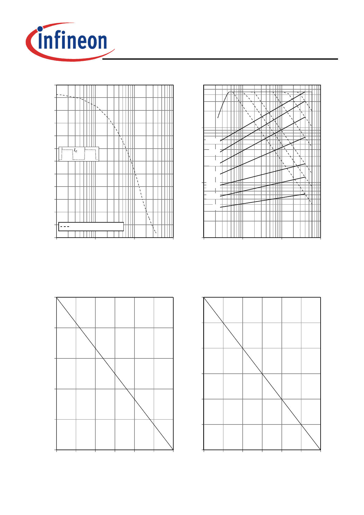
Figure 1.
Collectorcurrentasafunctionofswitching
frequency
(T
vj
≤
175°C,T
a
=55°C,D=0,5,V
CE
=400V,
V
GE
=15/0V,r
G
=15
Ω
,PCBmountingwith
thermal vias and heatsink, see Appnote:
www.infineon.com/igbt)
f,SWITCHINGFREQUENCY[kHz]
I
C
,COLLECTORCURRENT[A]
0.1
1
10
100
0
1
2
3
4
5
6
7
8
9
10
11
12
P
tot
=8,6W,R
th(j-a)
=8K/W
Figure 2.
Forwardbiassafeoperatingarea
(D=0,T
C
=25°C,T
vj
≤
175°C;V
GE
=15V)
V
CE
,COLLECTOR-EMITTERVOLTAGE[V]
I
C
,COLLECTORCURRENT[A]
1
10
100
1000
0.1
1
10
t
p
=1µs
10µs
20µs
50µs
200µs
500µs
DC
Figure 3.
Powerdissipationasafunctionofcase
temperature
(T
vj
≤
175°C)
T
C
,CASETEMPERATURE[°C]
P
tot
,POWERDISSIPATION[W]
25
50
75
100
125
150
175
0
50
100
150
200
250
Figure 4.
Collectorcurrentasafunctionofcase
temperature
(V
GE
≥
15V,T
vj
≤
175°C)
T
C
,CASETEMPERATURE[°C]
I
C
,COLLECTORCURRENT[A]
25
50
75
100
125
150
175
0
5
10
15
20
25
30
8
IKD15N60RA
TRENCHSTOP
TM
RC-Seriesforhardswitchingapplications
Rev.2.1,2013-02-15
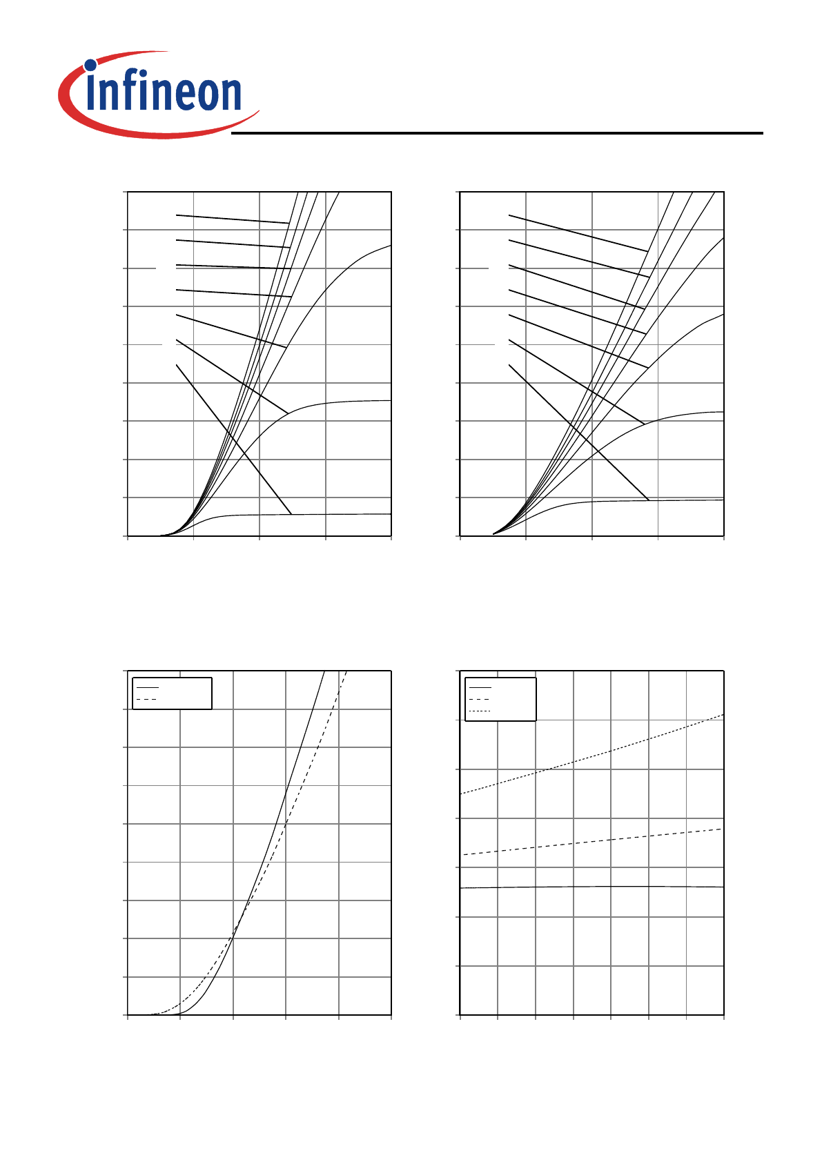
Figure 5.
Typicaloutputcharacteristic
(T
vj
=25°C)
V
CE
,COLLECTOR-EMITTERVOLTAGE[V]
I
C
,COLLECTORCURRENT[A]
0
1
2
3
4
0
5
10
15
20
25
30
35
40
45
V
GE
=20V
17V
15V
13V
11V
9V
7V
Figure 6.
Typicaloutputcharacteristic
(T
vj
=175°C)
V
CE
,COLLECTOR-EMITTERVOLTAGE[V]
I
C
,COLLECTORCURRENT[A]
0
1
2
3
4
0
5
10
15
20
25
30
35
40
45
V
GE
=20V
17V
15V
13V
11V
9V
7V
Figure 7.
Typicaltransfercharacteristic
(V
CE
=10V)
V
GE
,GATE-EMITTERVOLTAGE[V]
I
C
,COLLECTORCURRENT[A]
4
6
8
10
12
14
0
5
10
15
20
25
30
35
40
45
T
j
=25°C
T
j
=175°C
Figure 8.
Typicalcollector-emittersaturationvoltageas
afunctionofjunctiontemperature
(V
GE
=15V)
T
vj
,JUNCTIONTEMPERATURE[°C]
V
CEsat
,COLLECTOR-EMITTERSATURATION[V]
0
25
50
75
100
125
150
175
0.0
0.5
1.0
1.5
2.0
2.5
3.0
3.5
I
C
=7,5A
I
C
=15A
I
C
=30A
9
IKD15N60RA
TRENCHSTOP
TM
RC-Seriesforhardswitchingapplications
Rev.2.1,2013-02-15
Figure 9.
Typicalswitchingtimesasafunctionof
collectorcurrent
(inductiveload,T
vj
=175°C,V
CE
=400V,
V
GE
=15/0V,r
G
=15
Ω
,Dynamictestcircuitin
Figure E)
I
C
,COLLECTORCURRENT[A]
t,SWITCHINGTIMES[ns]
0
5
10
15
20
25
30
1
10
100
1000
t
d(off)
t
f
t
d(on)
t
r
Figure 10.
Typicalswitchingtimesasafunctionofgate
resistor
(inductiveload,T
vj
=175°C,V
CE
=400V,
V
GE
=15/0V,I
C
=15A,Dynamictestcircuitin
Figure E)
r
G
,GATERESISTOR[
Ω
]
t,SWITCHINGTIMES[ns]
0
10
20
30
40
50
1
10
100
1000
t
d(off)
t
f
t
d(on)
t
r
Figure 11.
Typicalswitchingtimesasafunctionof
junctiontemperature
(inductiveload,V
CE
=400V,V
GE
=15/0V,
I
C
=15A,r
G
=15
Ω
,Dynamictestcircuitin
Figure E)
T
vj
,JUNCTIONTEMPERATURE[°C]
t,SWITCHINGTIMES[ns]
25
50
75
100
125
150
175
1
10
100
1000
t
d(off)
t
f
t
d(on)
t
r
Figure 12.
Gate-emitterthresholdvoltageasafunction
ofjunctiontemperature
(I
C
=0,25mA)
T
vj
,JUNCTIONTEMPERATURE[°C]
V
GE(th)
,GATE-EMITTERTHRESHOLDVOLTAGE[V]
25
50
75
100
125
150
175
2
3
4
5
6
7
typ.
min.
max.
10
IKD15N60RA
TRENCHSTOP
TM
RC-Seriesforhardswitchingapplications
Rev.2.1,2013-02-15
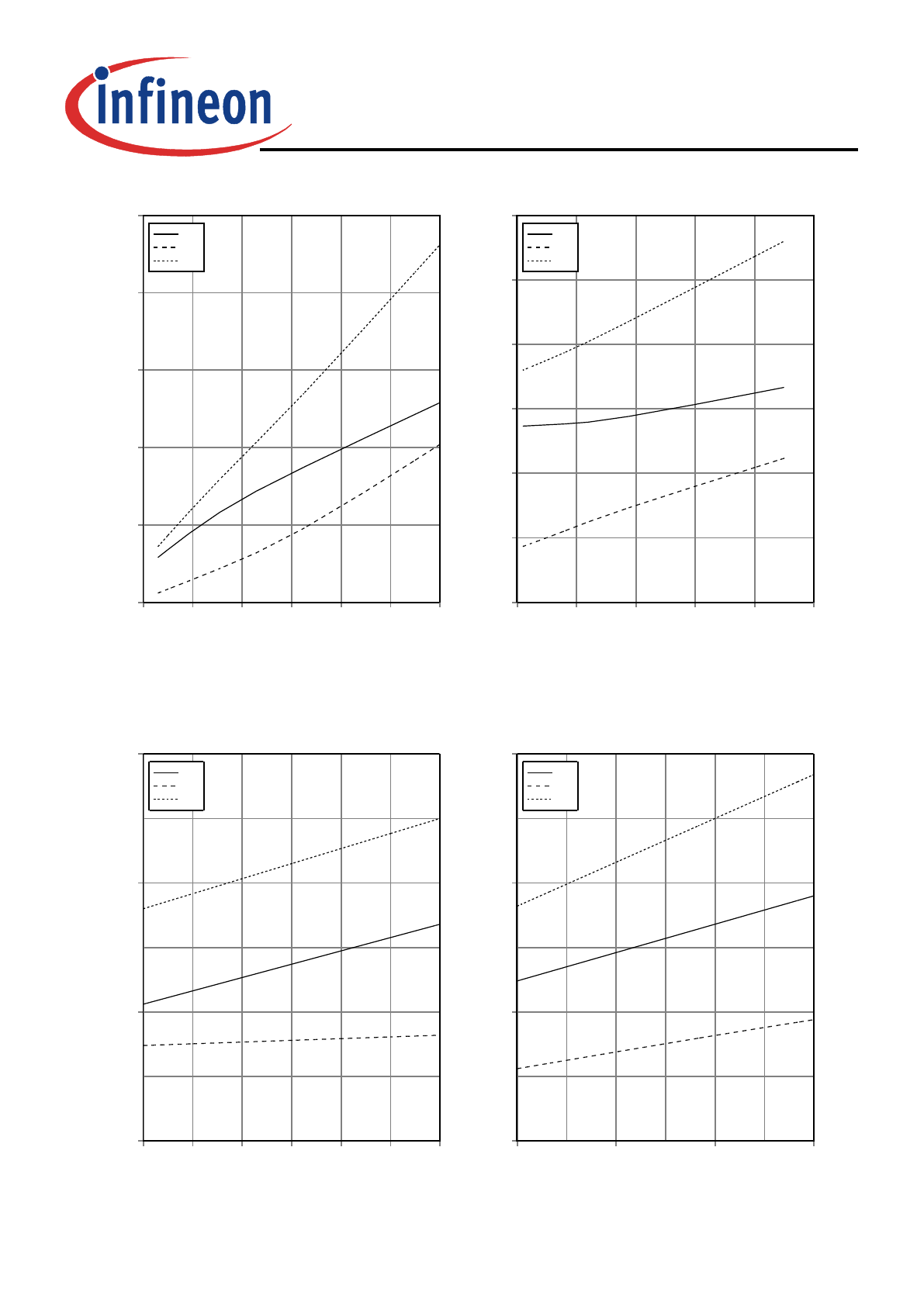
Figure 13.
Typicalswitchingenergylossesasa
functionofcollectorcurrent
(inductiveload,T
vj
=175°C,V
CE
=400V,
V
GE
=15/0V,r
G
=15
Ω
,Dynamictestcircuitin
Figure E)
I
C
,COLLECTORCURRENT[A]
E
,SWITCHINGENERGYLOSSES[mJ]
0
5
10
15
20
25
30
0.0
0.5
1.0
1.5
2.0
2.5
E
off
E
on
E
ts
Figure 14.
Typicalswitchingenergylossesasa
functionofgateresistor
(inductiveload,T
vj
=175°C,V
CE
=400V,
V
GE
=15/0V,I
C
=15A,Dynamictestcircuitin
Figure E)
r
G
,GATERESISTOR[
Ω
]
E
,SWITCHINGENERGYLOSSES[mJ]
0
10
20
30
40
50
0.0
0.3
0.6
0.9
1.2
1.5
1.8
E
off
E
on
E
ts
Figure 15.
Typicalswitchingenergylossesasa
functionofjunctiontemperature
(inductiveload,V
CE
=400V,V
GE
=15/0V,
I
C
=15A,r
G
=15
Ω
,Dynamictestcircuitin
Figure E)
T
vj
,JUNCTIONTEMPERATURE[°C]
E
,SWITCHINGENERGYLOSSES[mJ]
25
50
75
100
125
150
175
0.0
0.5
1.0
1.5
E
off
E
on
E
ts
Figure 16.
Typicalswitchingenergylossesasa
functionofcollectoremittervoltage
(inductiveload,T
vj
=175°C,V
GE
=15/0V,
I
C
=15A,r
G
=15
Ω
,Dynamictestcircuitin
Figure E)
V
CE
,COLLECTOR-EMITTERVOLTAGE[V]
E
,SWITCHINGENERGYLOSSES[mJ]
300
350
400
450
0.0
0.5
1.0
1.5
E
off
E
on
E
ts